
For several leading quantum-computing approaches—especially trapped ions and neutral atoms—lasers aren’t just “support equipment”. They’re part of the control plane: used to cool atoms, prepare quantum states, drive logic gates and read out results. That means the lasers’ frequencies (their colours) must be held rock-steady and set precisely, often across multiple wavelengths, sometimes with tight timing requirements as well.
In practice, those demands have pushed research labs towards bulky optical benches packed with stabilisation hardware. According to the University of Colorado Boulder report on the new device, today’s high-performance laser-frequency control commonly relies on benchtop instruments that can be power-hungry and finicky—fine for a few qubits in a lab, but a headache for building machines with orders of magnitude more qubits.
That’s the context for CU Boulder’s claim: if you can shrink the laser-control stack to something closer to a chip module—while keeping precision—you remove one of the less glamorous but very real blockers to scaling.
The CU Boulder device, in plain terms
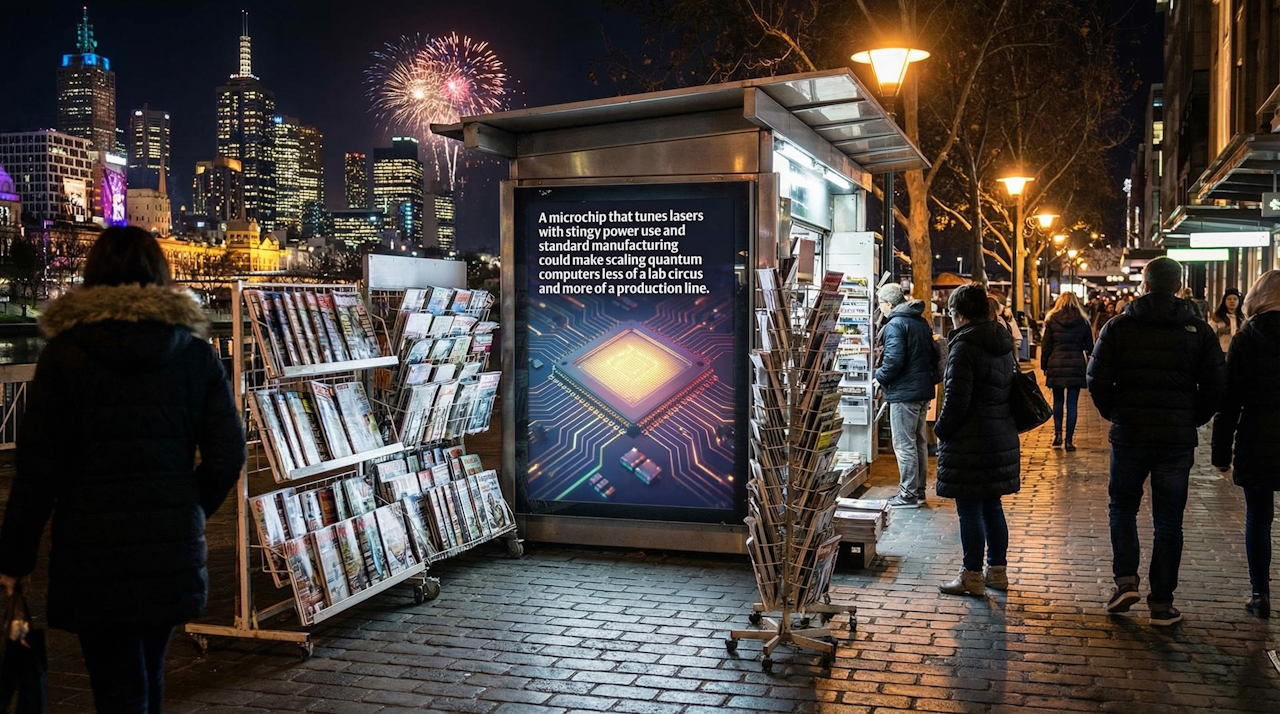
The headline result, as described in CU Boulder’s public materials, is a microchip-sized component that can control laser frequencies with “extreme precision” while using far less power than conventional setups, and that can be made with standard chip-manufacturing processes rather than bespoke optical assembly. Those points are laid out in CU Boulder’s own write-up and in syndicated coverage, including ScienceDaily’s summary.
The reporting positions the chip as a way to replace (or substantially reduce dependence on) racks of equipment used for frequency stabilisation and tuning. While the public-facing pieces focus on the “what” more than the full engineering “how”, the significance is straightforward: frequency control is typically achieved by referencing a laser to a stable optical standard and actively correcting drift. Doing that in a compact, low-power form factor is difficult because you’re fighting thermal noise, vibration sensitivity and electronic noise—problems that are often easier to manage on an optical bench than in a package the size of a fingernail.
CU Boulder’s work sits within a broader push in “integrated photonics”: moving optics functions onto chips in much the same way electronics went from discrete components to integrated circuits. In quantum engineering, that shift is often framed as a pathway from laboratory setups towards more product-like systems, though the outcome depends on successful integration and manufacturing.
Precision without the power bill
Power use matters in quantum computing for reasons that aren’t always obvious. It’s not just electricity cost; it’s what power becomes: heat, stray electromagnetic noise, and mechanical vibration from fans and cooling systems. These factors can complicate the thermal and environmental management that many quantum platforms already require.
CU Boulder’s reports emphasise that the chip achieves laser-frequency control with far less power than “today’s bulky systems”. If that advantage holds up through engineering and packaging, it could ease several constraints at once: lower thermal load near sensitive hardware, simpler system-level cooling, and potentially denser layouts where control modules can sit closer to the lasers and optical distribution network.
It’s also relevant to reliability. Bench-top stabilisation can be exquisitely precise, but it can also be sensitive to alignment drift and environmental disturbances. A chip-scale implementation, by contrast, can be mechanically rigid and reproducible—though it may also introduce new failure modes, such as packaging stress or chip-to-chip variation. The promise here is not that the underlying physics becomes easy, but that parts of the hardware could become more repeatable.
Standard fabrication: the scaling lever
Perhaps the most consequential line in the coverage is the claim that the device is made using standard chip manufacturing, which implies the design could be reproduced at scale rather than individually crafted. That’s the difference between a clever instrument and a potentially enabling technology.
The CU Boulder piece explicitly flags manufacturability: using “standard chip manufacturing” instead of custom-built systems. In the semiconductor world, that phrase carries weight: it can suggest a pathway to volume production, tighter tolerances through mature process control, and cost declines through learning curves. Not every photonics device fits neatly into mainstream fabrication flows, and not every lab prototype survives the move to industrial process design kits (PDKs). But if this one does, it could help quantum hardware teams reduce their reliance on highly customised laser-control assemblies.
This matters for quantum companies trying to scale beyond a handful of demonstration machines. The goal is to make it feasible to build far larger quantum systems than are practical with today’s room-filling, manually tuned optics. That’s an engineering statement more than a theoretical one: reducing size, weight, power and alignment overhead could turn “more qubits” from a laboratory ambition into a manufacturing and supply-chain challenge—one that the electronics industry has historically been effective at addressing.
What it could unlock (and what it won’t)
If laser-frequency control becomes chip-scale, several second-order effects become plausible:
- More channels without more benches. Many atom-based architectures need multiple stabilised lasers. A chip approach could make it easier to replicate those channels, supporting larger arrays or more parallel operation.
- Tighter integration of control stacks. Shorter optical paths and integrated modules can reduce sensitivity to environmental noise, potentially improving stability—though the net gain depends on packaging and system design.
- Faster deployment and servicing. Swapping a module may be easier than re-aligning a bench. That’s valuable if quantum computers are to run outside specialist labs.
But it’s also worth being sober about what’s not solved by a single chip. Quantum computers still face major hurdles in qubit quality, error correction overheads, cryogenics (for some platforms), vacuum systems (for many atom/ion platforms), and software tooling. Laser stabilisation is an important piece, not the whole puzzle.
There’s also a translation gap between a research demonstration and an operational subsystem. The press materials highlight power and precision; less visible are the practical questions product teams typically ask next: How robust is it to temperature swings? How is it packaged and fibre-coupled? What are the long-term drift characteristics? How does it behave under vibration? Can it be calibrated in the field? These are generally solvable questions, but they often determine whether the technology becomes a standard module or remains a specialised component.
The wider trend: microcombs and on-chip frequency references
CU Boulder’s announcement lands in a decade-long trend towards on-chip frequency tools, including optical frequency combs and microresonator-based systems used as stable references. These technologies are well established in precision metrology and are increasingly being explored for communications and sensing.
For readers wanting a grounded reference point, the US National Institute of Standards and Technology overview of optical frequency combs explains how combs act like “rulers” for light—linking optical frequencies to more easily measured microwave references. Meanwhile, broader technical context on chip-based combs and frequency synthesis is summarised in the peer-reviewed literature, such as a Nature Photonics review on microcombs. Not every chip-scale frequency controller is a comb, but the direction of travel is similar: take what used to require a table of optics and make it manufacturable.
That matters for quantum because atom-based qubits often depend on precisely tuned optical transitions. If stable, well-referenced light sources can be produced and controlled with integrated hardware, the control layer for quantum machines may start to resemble more mature photonics industries, rather than bespoke laboratory infrastructure.
What to watch next in 2026
The most immediate questions are about follow-through: independent replication, performance numbers in operational environments, and integration into real quantum control stacks.
Three milestones would help indicate whether this “tiny chip” is genuinely transformative rather than merely impressive:
- System demonstrations, not just component demos. Showing the chip running alongside lasers in a quantum experiment, maintaining stability over long periods.
- Manufacturing proof. Evidence that the device can be fabricated across wafers with predictable yield and that performance is consistent across chips.
- Packaging and deployment. A credible route to rugged modules—fibre-coupled, thermally managed, and serviceable—because packaging is often where integrated photonics projects stumble.
If those steps land, CU Boulder’s work could become one of those quietly pivotal technologies: not the qubits themselves, but the industrialised infrastructure that makes larger-scale quantum systems more practical.
In the near term, the chip is best viewed as a potential scaling lever—reducing power, size and complexity in laser-frequency control. If quantum computing is to move from carefully tended prototypes to machines built in quantity, that kind of unglamorous integration could be one of the changes that meaningfully shifts the economics and operability of the field.